Eshylon Temporary Bonding
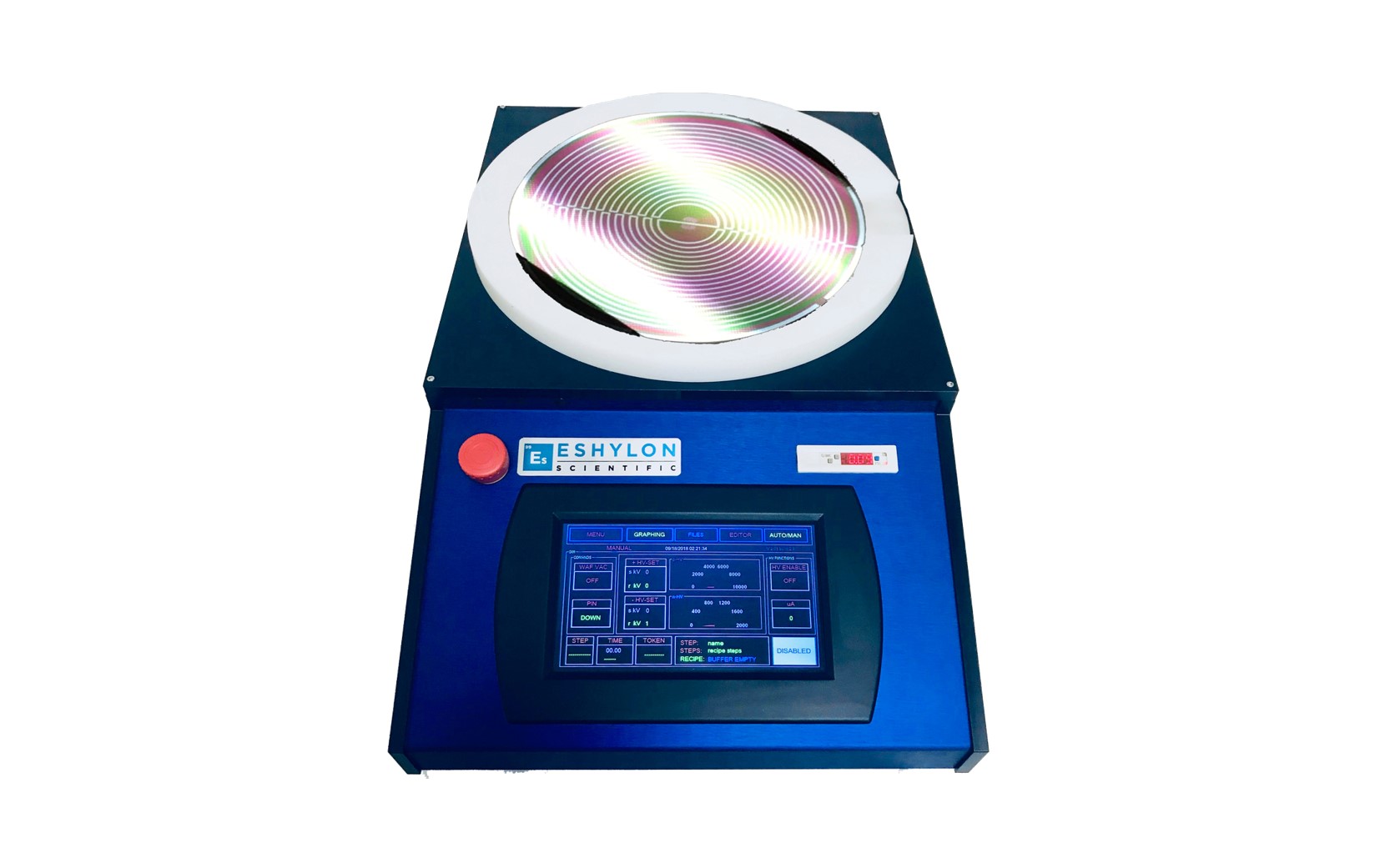
Eshylon MESC
Model:
Temporary bonding has emerged as a mission-critical application for production of today's advanced devices in Semiconductor, Automotive, Defense, Quantum Computing, Biomedical and other industries.
Eshylon's new, patented Mobile Electrostatic Carrier (MESC) platform enables leading-edge device fabrication by providing a rigid but mobile platform for handling challenging substrates in an R&D, pilot line or high volume manufacturing environment.
Utilizing electrostatic forces, Eshylon carriers can bond in seconds to a target substrate for processing then release the substrate gently without the need for additional clean steps or adhesives, all on a single tool.
Facility Bridge (Multiple Size Substrates)
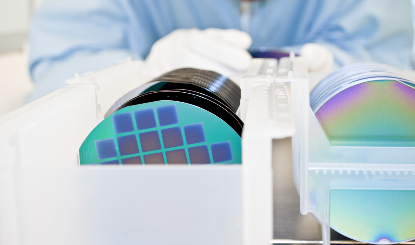
Traditional production tools are configured and optimized for standardized wafers ranging from 100mm to 300mm, and can only process one wafer size without significant costly upgrades. Eshylon MESCs overcome this limitation, enabling dramatic ROI through reuse of 300mm or 200mm tool sets for smaller substrates bonded to Eshylon carriers.
HIGHLIGHTS
Reuse of any pre-existing toolset for small substrate handling
Available in identical form factor of all SEMI-specified silicon wafer sizes
Rapid & versatile conversion of existing capital equipment to new handling requirements
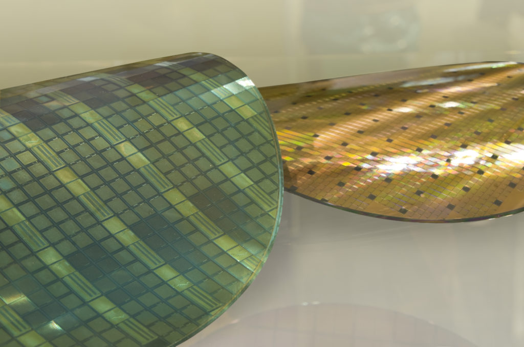
Thin Wafer Handling
With mobile devices forcing miniaturization of packaged ICs, device thickness must be reduced dramatically. Backside thinning of ultra-thin and delicate substrates presents serious wafer handling challenges that Eshylon solves. Good bye breakage, low yields and slow throughput.
HIGHLIGHTS
Fast, high throughput processing with instant, delicate release
Variable bonding voltage to optimize bonding and release of thin or delicate 3/5 materials
High yields and extraordinarily versatile handling applications
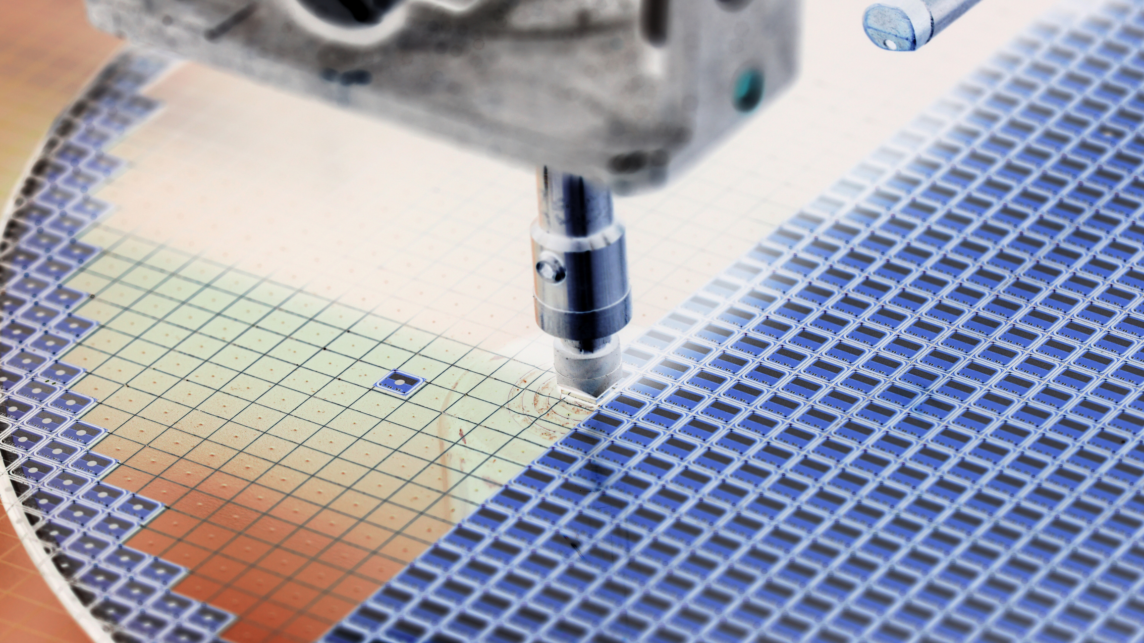
Device Packaging
With 2.5 and 3D packaging applications, device handling challenges have diversified. Eshylon has experience with development of custom packaging-handling applications and form factors, providing application-specific mobile device carriers that can be used in applications such as:
HIGHLIGHTS
Reflow
Plasma and flux cleaning
Loading & unloading into pick-and-place tools
Various other high-temperature cure processes